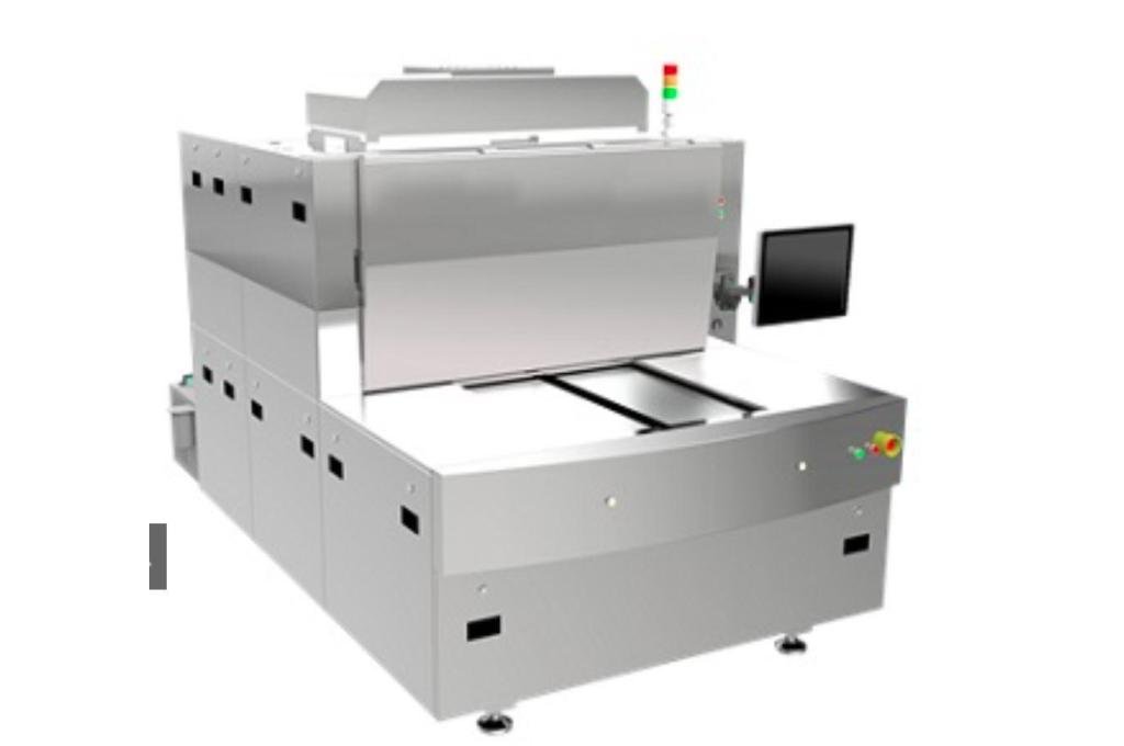
PCB Solder Mask LDI Exposure Machine is a high-precision Laser Direct Imaging (LDI) system designed for solder mask exposure and advanced PCB manufacturing. By replacing traditional phototool-based exposure with digital laser imaging, it delivers superior alignment accuracy, higher resolution, improved production efficiency, and exceptional image consistency.
The machine is ideal for high-volume PCB production, supporting automatic image compensation, precise multilayer alignment, and seamless integration with modern smart manufacturing systems.
The PCB Solder Mask LDI Exposure Machine uses a high-power 405 nm laser source to directly expose solder mask patterns onto printed circuit boards without the need for photographic films. Digital imaging technology eliminates common issues associated with conventional exposure methods, including film distortion, temperature and humidity sensitivity, and alignment inaccuracies.Designed for advanced PCB fabrication, the system offers high-speed processing, automatic expansion and contraction compensation, and excellent registration accuracy for fine-line circuit production.
Laser Direct Imaging (LDI) technology
High-speed solder mask exposure
Film-free digital imaging process
High-resolution laser exposure
Automatic expansion and contraction
| Parameter | Specification |
|---|---|
| Model | ADI-ST-650 |
| Table Type | Single Table |
| Loading Method | Manual |
| Maximum Substrate Size | 635 × 820 mm |
| Maximum Exposure Area | 630 × 810 mm |
| Minimum Substrate Size | 200 × 170 mm |
| PCB Thickness | 0.075–5.0 mm (Expandable to 8.0 mm) |
| Laser Wavelength | 405 ±5 nm |
| Laser Power | 30 W |
| Exposure Energy Range | 5–2000 mJ |
| Energy Uniformity | ≥95% |
| Overall Dimensions | 2600 × 1750 × 1970 mm |
| Machine Weight | Approximately 4000 kg |
| Parameter | Specification |
|---|---|
| Minimum Resolution | 35 μm / 35 μm |
| Recommended Production Line Width | ≥50 μm (2.5 mil or above) |
| Depth of Focus | ±300 μm |
| Line Width Tolerance | ±10% |
| Alignment Accuracy | ±12 μm |
| Interlayer Alignment Accuracy | 24 μm |
| Number of Exposure Shots | 6 |
| Exposure Condition | Processing Speed |
|---|---|
| 35 mJ, 3 mil | Approximately 10 seconds per side |
| 100 mJ, 3 mil | Approximately 20 seconds per side |
Processing times exclude PCB loading and unloading.
The machine supports direct import of industry-standard PCB manufacturing files, including:
Gerber 274D
Gerber 274X
ODB++
One-click data import simplifies production preparation and reduces programming time.
Read morePCB Solder Mask LDI Exposure Machine is a high-precision Laser Direct Imaging (LDI) system designed for solder mask exposure and advanced PCB manufacturing. By replacing traditional phototool-based exposure with digital laser imaging, it delivers superior alignment accuracy, higher resolution, improved production efficiency, and exceptional image consistency.
The machine is ideal for high-volume PCB production, supporting automatic image compensation, precise multilayer alignment, and seamless integration with modern smart manufacturing systems.
The PCB Solder Mask LDI Exposure Machine uses a high-power 405 nm laser source to directly expose solder mask patterns onto printed circuit boards without the need for photographic films. Digital imaging technology eliminates common issues associated with conventional exposure methods, including film distortion, temperature and humidity sensitivity, and alignment inaccuracies.Designed for advanced PCB fabrication, the system offers high-speed processing, automatic expansion and contraction compensation, and excellent registration accuracy for fine-line circuit production.
Laser Direct Imaging (LDI) technology
High-speed solder mask exposure
Film-free digital imaging process
High-resolution laser exposure
Automatic expansion and contraction
| Parameter | Specification |
|---|---|
| Model | ADI-ST-650 |
| Table Type | Single Table |
| Loading Method | Manual |
| Maximum Substrate Size | 635 × 820 mm |
| Maximum Exposure Area | 630 × 810 mm |
| Minimum Substrate Size | 200 × 170 mm |
| PCB Thickness | 0.075–5.0 mm (Expandable to 8.0 mm) |
| Laser Wavelength | 405 ±5 nm |
| Laser Power | 30 W |
| Exposure Energy Range | 5–2000 mJ |
| Energy Uniformity | ≥95% |
| Overall Dimensions | 2600 × 1750 × 1970 mm |
| Machine Weight | Approximately 4000 kg |
| Parameter | Specification |
|---|---|
| Minimum Resolution | 35 μm / 35 μm |
| Recommended Production Line Width | ≥50 μm (2.5 mil or above) |
| Depth of Focus | ±300 μm |
| Line Width Tolerance | ±10% |
| Alignment Accuracy | ±12 μm |
| Interlayer Alignment Accuracy | 24 μm |
| Number of Exposure Shots | 6 |
| Exposure Condition | Processing Speed |
|---|---|
| 35 mJ, 3 mil | Approximately 10 seconds per side |
| 100 mJ, 3 mil | Approximately 20 seconds per side |
Processing times exclude PCB loading and unloading.
The machine supports direct import of industry-standard PCB manufacturing files, including:
Gerber 274D
Gerber 274X
ODB++
One-click data import simplifies production preparation and reduces programming time.

 Pro
Jinan chanke mechanical equipment co.,ltd
Pro
Jinan chanke mechanical equipment co.,ltd

 Pro
Wuxi Hairui Welding & Cutting Equipment Manufacturing Co., Ltd.
Pro
Wuxi Hairui Welding & Cutting Equipment Manufacturing Co., Ltd.
 Pro
Wuxi Hairui Welding & Cutting Equipment Manufacturing Co., Ltd.
Pro
Wuxi Hairui Welding & Cutting Equipment Manufacturing Co., Ltd.
 Pro
Wuxi Hairui Welding & Cutting Equipment Manufacturing Co., Ltd.
Pro
Wuxi Hairui Welding & Cutting Equipment Manufacturing Co., Ltd.
 Pro
Wuxi Hairui Welding & Cutting Equipment Manufacturing Co., Ltd.
Pro
Wuxi Hairui Welding & Cutting Equipment Manufacturing Co., Ltd.
 Pro
Wuxi Hairui Welding & Cutting Equipment Manufacturing Co., Ltd.
Pro
Wuxi Hairui Welding & Cutting Equipment Manufacturing Co., Ltd.
 Pro
Jinan Jiedi Motorcycle Technology Co., Ltd.
Pro
Jinan Jiedi Motorcycle Technology Co., Ltd.
 Pro
OPPAIR Machinery
Pro
OPPAIR Machinery

 Pro
GBOS LASER INC.
Pro
GBOS LASER INC.
 Pro
GBOS LASER INC.
Pro
GBOS LASER INC.
 Pro
GBOS LASER INC.
Pro
GBOS LASER INC.
 Pro
GBOS LASER INC.
Pro
GBOS LASER INC.
 Pro
GBOS LASER INC.
Pro
GBOS LASER INC.
 Pro
Jiangsu Weiyang Heavy Industry Technology Co., Ltd.
Pro
Jiangsu Weiyang Heavy Industry Technology Co., Ltd.
 Pro
Jiangsu Weiyang Heavy Industry Technology Co., Ltd.
Pro
Jiangsu Weiyang Heavy Industry Technology Co., Ltd.

 Pro
ANHUI DONGHAI MACHINE TOOL CO., LTD.
Pro
ANHUI DONGHAI MACHINE TOOL CO., LTD.
 Pro
ANHUI DONGHAI MACHINE TOOL CO., LTD.
Pro
ANHUI DONGHAI MACHINE TOOL CO., LTD.
 Pro
ANHUI DONGHAI MACHINE TOOL CO., LTD.
Pro
ANHUI DONGHAI MACHINE TOOL CO., LTD.
 Pro
ANHUI DONGHAI MACHINE TOOL CO., LTD.
Pro
ANHUI DONGHAI MACHINE TOOL CO., LTD.
 Pro
ANHUI DONGHAI MACHINE TOOL CO., LTD.
Pro
ANHUI DONGHAI MACHINE TOOL CO., LTD.

 Pro
Jieyimei Laser Technology
Pro
Jieyimei Laser Technology
 Pro
Jieyimei Laser Technology
Pro
Jieyimei Laser Technology
 Pro
Jieyimei Laser Technology
Pro
Jieyimei Laser Technology
 Pro
Jieyimei Laser Technology
Pro
Jieyimei Laser Technology


 Welcome!